
Our Services
Advanced Photon Sciences offers both products and technology to solution your innovation. We have assembled a team of designers which has skill sets ranging from developing lab processes, mechanical designs and 3-D prototypes to ASIC and computer memory design.
Fabrication
Mini- CNC and CNC lathe, 90W laser engraver / cutter with roll to roll feed stock capabilities, Electronics, and metal shop.
Consulting: Technical, Business, IP
Program Management
DESIGN / BUILD / SYSTEMS
Research and Development
Product Development
Concept -> Prototype -> Pre-Production -> Manufacturing
Our engineers and scientists have roots in high volume manufacturing, and know how to design highly compatible products for simple reliable fabrication. Craftsmen in their trades, as Vermonters, we pride ourselves in Yankee ingenuity.
Specification
Design
Manufacturing
Testing
Prototyping and Process development
Our newly completed Mini-Fab with three different process zones Lithography, Process, Electronics and wafer probing, (class 100-1000 clean room), we are able to perform semiconductor processing and metrology using high resolution Scanning Electron Microscope, SEM (Back scatter and Secondary electron detectors), as well as high magnification Optical and inspection microscopes. Pattern generation using the SEM with resolution down below 50nm on smaller test samples, and as small as 400nm on full 200mm wafers, including irregularly shapes substrates. Metal and Oxide deposition using sputtered, and Atomic Layer Deposition, ALD. Dry etching (RIE) Reactive Ion Etch. Electronics testing and design. Complete electronics test gear setup with parametric analyzers, and 300mm capable wafer probe station.
Monolayer Coating Systems
APS offers The revolutionary VfX-100 coating system from VersufleX Technologies. This amazing system is able to coat monolayers of a wide range of nano and micro scaled particles as well as polymers.
Ultra-thin coatings and mono-layer coatings
Equipment Design
Equipment Build
Our Capabilities
APS offers a variety of Scientific, Application, and Design Engineering services. Our professionals have been working together for over a decade on everything from advanced product design to basic proof of concept research and systems.
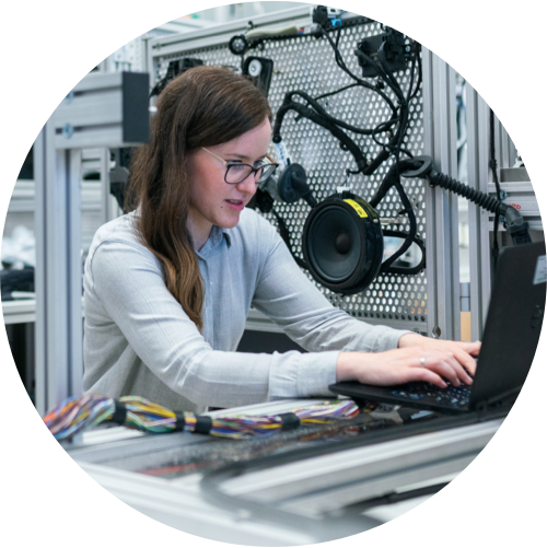
Let APS staff your short and long term needs with just the right skill for the job.
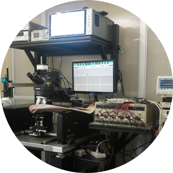
A variety of advanced instruments allows our team to provide detailed testing and analysis services.

Advanced packaging design, custom circuit design, embedded logic and control systems
Some of our unique capabilities include
Atomic Layer Deposition, ALD
Metal and Dielectric sputtering
High resolution direct write Lithography,
100nm e-beam on 100mm substrates
400nm on 200mm substrates (DLP Optical 385nm)
High power short burst laser systems
Product Design
Optics Design and Testing
Custom circuit design; multi-layered PCB and surface mount technologies
Wafer probe testing
ASIC circuit design Clewin and DW-2000 workshop
Mechanical design and advanced machined part capability
Fusion, FEA, Solid modeling
Applications development and support
Field service and customer support
Soldier personal protective gear (eye wear)
Industrial controls and automation
Reporting and production compliance
Custom Research Machines and Systems
Laboratory, R&D, Production & Manufacturing systems including semiconductor-based systems